-
09-06-2017
Fast growth of inch-sized single-crystalline graphene from a controlled single nucleus on Cu-Ni alloys
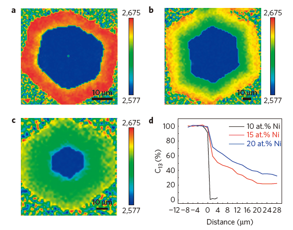
Wafer-scale single-crystalline graphene monolayers are highly sought after as an ideal platform for electronic and other applications (1-3). At present, state-of-the-art growth methods based on chemical vapour deposition allow the synthesis of one-centimeter-sized single-crystalline graphene domains similar to 12 h, by suppressing nucleation events on the growth substrate (4). Here we demonstrate an efficient strategy for achieving large-area single-crystalline graphene by letting a single nucleus evolve in a monolayer at a fast rate. By locally feeding carbon precursors to a desired position of a substrate composed of an optimized Cu-Ni alloy, we synthesized an similar to 1.5-inch-large graphene monolayer in 2.5 h. Localized feeding ind...[ Learn more ]
-
09-06-2017
Information Functional Materials State Key Laboratory of the fifth session of the four academic committee was success...
-
09-06-2017
6.2-GHz modulated terahertz light detection using fast terahertz quantum well photodetectors
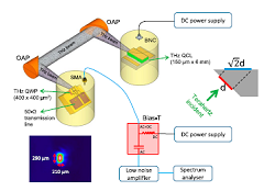
The fast detection of terahertz radiation is of great importance for various applications such as fast imaging, high speed communications, and spectroscopy. Most commercial products capable of sensitively responding the terahertz radiation are thermal detectors, i.e., pyroelectric sensors and bolometers. This class of terahertz detectors is normally characterized by low modulation frequency (dozens or hundreds of Hz). Here we demonstrate the first fast semiconductor-based terahertz quantum well photodetectors by carefully designing the device structure and microwave transmission line for high frequency signal extraction. Modulation response bandwidth of gigahertz level is obtained. As an example, the 6.2-GHz modulated terahertz light emi...[ Learn more ]
-
09-06-2017
Homogeneous spectral spanning of terahertz semiconductor lasers with radio frequency modulation
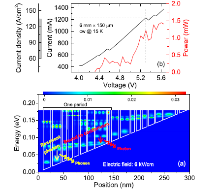
Homogeneous broadband and electrically pumped semiconductor radiation sources emitting in the terahertz regime are highly desirable for various applications, including spectroscopy, chemical sensing, and gas identification. In the frequency range between 1 and 5 THz, unipolar quantum cascade lasers employing electron inter-subband transitions in multiple-quantum-well structures are the most powerful semiconductor light sources. However, these devices are normally characterized by either a narrow emission spectrum due to the narrow gain bandwidth of the inter-subband optical transitions or an inhomogeneous broad terahertz spectrum from lasers with heterogeneous stacks of active regions. Here, we report the demonstration of homogeneous spe...[ Learn more ]
-
09-06-2017
Nanoscale distribution of Bi atoms in InP1-xBix
The nanoscale distribution of Bi in InPBi is determined by atom probe tomography and transmission electron microscopy. The distribution of Bi atoms is not uniform both along the growth direction and within the film plane. A statistically high Bi-content region is observed at the bottom of the InPBi layer close to the InPBi/InP interface. Bi-rich V-shaped walls on the (-111) and (1–11) planes close to the InPBi/InP interface and quasi-periodic Bi-rich nanowalls in the (1–10) plane with a periodicity of about 100 nm are observed. A growth model is proposed to explain the formation of these unique Bi-related nanoscale features. These features can significantly affect the deep levels of the InPBi epilayer. The regions in the InPBi layer wi...[ Learn more ]


