3D Electron Beam Lithography Technology
Date:16-09-2021 | 【Print】 【close】
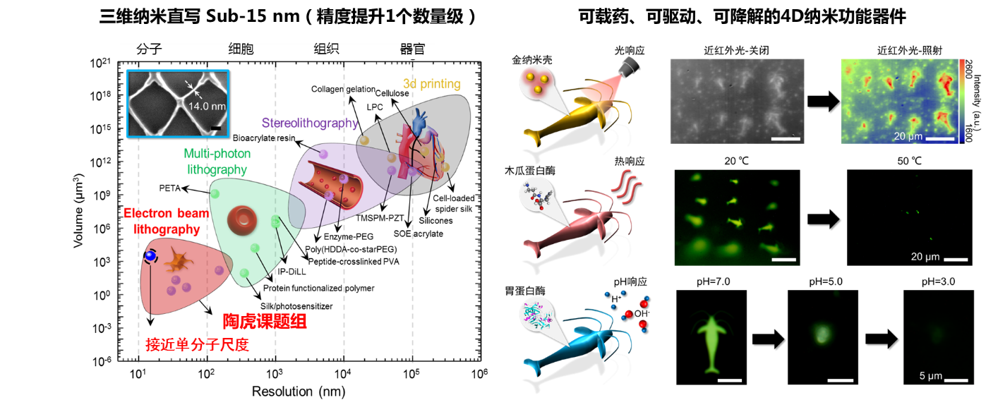
Electron beam lithography (EBL) represents the smallest and finest practical patterning tool and still remains the method of choice for fabricating two-dimensional (2D) nanometer-scale structures. How to expand the high precision of EBL to true three-dimensional (3D) nanofabrication has been the main goal of researchers in the recent decades.
Compared with conventional EBL, which uses high voltage (tens of kV) and thin photoresist (tens of nanometers) to ensure the alignment and resolution of lithography, Professor Tiger H. Tao and colleagues at SIMIT (Shanghai Institute of Microsystem and Information Technology, Chinese Academy of Sciences) focus on the low voltage (several kV) EBL of thick photoresist (several microns). In cooperation with Professors Xiao-xia Xia and Zhi-gang Qian from Shanghai Jiao Tong University, they innovated and developed a series of bio-photoresist in genetically engineered spider silk protein with optimized gene sequence and molecular weight, and further investigated the millions of electrons behaviors in the spider silk layer with Monte Carlo modeling. The ability of regulating the penetration depth, termination position and energy dissipation of electrons in silk protein photoresist by tuning the accelerating voltage, allows the direct writing of true 3D nanostructures with molecular accuracy. The fabrication resolution of this 3D EBL technology can reach ~14 nm, which is close to the single molecule size of natural silk protein (~10 nm), an order of magnitude higher than the previous methods. The excellent mechanical strength of spider silk protein provides key support for complex 3D nanostructures. Combined with the good biocompatibility and further functionalization, a few sets of drug loaded, dynamic and degradable 4D functional nanodevices have been successfully fabricated and offer new opportunities for the research of intelligent bionic sensing, drug delivery nanorobotics, organoids-on-chips and so on.
The paper entitled “3D electron-beam writing at sub-15 nm resolution using spider silk as a resist”has been published in Nature Communications (DOI : 10.1038/s41467-021-25470-1). This work was supported by National Science and Technology Major Project from the Minister of Science and Technology of China, National Science Fund for Excellent Young Scholars, National Natural Science Foundation of China, Shanghai Outstanding Academic Leaders Plan, Shanghai Sailing Program, Key Research Program of Frontier Sciences, CAS and the Scientific Instrument Developing Project of the Chinese Academy of Sciences.
So far, Professor Tiger H. Tao's team has fundamentally established a complete set of 2D and 3D micro/nano fabrication technologies for silk protein, including 2D & 3D electron beam lithography, 2D & 2.5D ion beam lithography, 2D UV lithography, 2D near-field lithography, 2D & 3D soft lithography, 2D & 3D nano imprinting, 2D & 3D self-assembly and 2D inkjet printing, covering nano, micron to millimeter and wafer scale. It guarantees the gorgeous transformation of silk protein from traditional textile materials to medical materials, and then to integrated circuit (IC) and sensor materials.
Paper link: https://www.nature.com/articles/s41467-021-25470-1
| 附件下载: |