Top Ten Achievements of Optics in China in 2019 :Realization of Wafer-Scale Nanogratings with Sub-50 nm period through Vacancy Epitaxy
Date:20-03-2020 | 【Print】 【close】
The group of professor Xin Ou from Shanghai Institute of Microsystem and Information Technology, Chinese Academy of Sciences, and collaborators from Tongji University have demonstrated a novel method for fabricating large-scale ultrahigh line density nanogratings. The line density of the prepared grating devices on 2 inch wafer is more than 20000 lines / mm. Combining with high efficiency X-ray multilayer film, the experimental dispersion performance is 6 times higher than the state of the art highest linear density grating (5000 lines / mm) made by conventional nanopatterning technologies. This new technology has been authorized by three Chinese patents and one German patent. It has been selected as top ten achievements of optics in China in 2019 recently released by Chinese Laser Press.

Fig.1 Schematic diagram of fabrication of multilayer film nanogratings (a-c)Cross sectional TEM images of Mo/Si (d,e) and Cr/C (f,g) multilayer film nanogratings
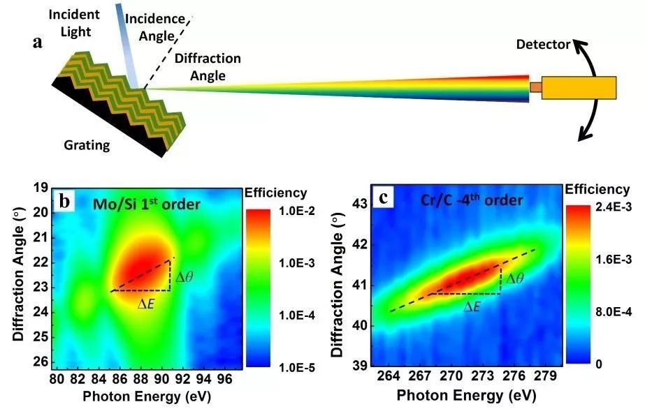
Fig.2 Dispersion test results of Mo/Si and Cr/C multilayer film nanogratings