Shanghai Institute of Microsystem and Information Technology, Chinese Academy of Sciences successful prepared graphene nanoribbons in hexagonal boron nitride trenches
Date:31-08-2017 | 【Print】 【close】
Shanghai Institute of Microsystem and Information Technology made important progress in the controlled preparation study of graphene nanoribbons. Researcher Wang Haimin’s team of State Key Laboratory of Functional Materials for Informatics achieved controlled growth of graphene nanoribbons in hexagonal boron nitride trenches for the first time internationally, successfully opened the graphene bandgap, and verified its excellent electrical properties at room temperature, which provided a possible technical path for the development of graphene digital circuit. The research findings were published in the journal Nature Communications on Mar 9, 2017 (L. Chen, et al, Oriented graphene nanoribbons embedded in hexagonal boron nitride trenches, Nature Communications, 8, 14703,DOI: 10.1038/ncomms14703 (2017)). The graphene nanoribbon preparation method proposed in this study has obtained invention patent in China and US.
The researchers first etched the hexagonal boron nitride monocrystal substrate by metal nanoparticles, cut out the thickness of monoatom layer, with flat edge, along the zigzag direction, and nano trenches with certain controllable width, and then prepared high-quality graphene nanoribbons with the length up to several microns and width of less than 10 nanometers in the trenches through the chemical vaporous deposition method. The experimental results showed that the graphene grew in the trenches by means of step epitaxy, and formed lattice constant in-plane heterojunction with the top hexagonal boron nitride. The researchers prepared a field-effect transistor based on graphene nanoribbons. The current switching ratio of the sub-5nm device at room temperature was greater than 104, the carrier mobility was about 750 cm2/Vs, and the electrical transport bandgap extracted from the electrical measurement was about 0.5eV, which could meet the basic requirements of digital circuit research and development.
Graphene is a two-dimensional atomic crystal composed of monolayer carbon atoms, with excellent physical, chemical and electrical properties. However, the bandgap of the intrinsic graphene material is zero, which has limited its application in micro-nanoelectronic devices, especially in digital circuits. It is a very promising method to prepare the graphene nanoribbons and opening the bandgap. However, the traditional graphene nanoribbon preparation method has problems in terms of width and boundary chirality control, and also faces the defect of the need for transfer. This study verified a kind of transfer-free, width and boundary controllable technical path on the ideal grapheme substrate of hexagonal boron nitride monocrystal, which provided in important platform for further exploration of graphene logic circuit compatible with CMOS integrated circuits.
The boundary controllability is an important prerequisite for the preparation of practical graphene logic devices. This study confirmed that the prepared nanoribbons had pure zigzag boundary structure through a variety of experimental methods. The studies on the direct evidence of atomic level element resolution are in progress.
This study was supported by the National Science and Technology Major Project 02 of the Ministry of Science and Technology "Wafer grade graphene electronic materials and devices research" (Grant No. 2011ZX02707) and other projects. Research cooperation units include ShanghaiTech University, Huazhong University of Science and Technology, Central South University, Nanyang Technological University, Fudan University and Shanghai Institute of Technical Physics of the Chinese Academy of Sciences.
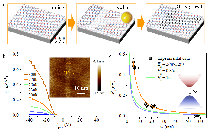
Fig. 1, a) Diagram of the preparation of zigzag-oriented graphene nanoribbons embedded in hexagonal boron nitride; b) Room temperature transport curve of field effect device of sub-5nm wide nanoribbon devices; c) Figure of the relation of bandgap energy gap and width of graphene nanoribbons
| 附件下载: |