-
C3N—A 2D Crystalline, Hole-Free, Tunable-Narrow-Bandgap Semiconductor with Ferromagnetic Properties
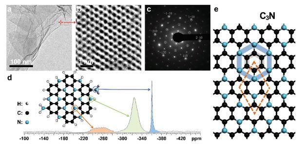
Here the authors report on the controllable large-scale synthesis of C3N, a 2D crystalline, hole-free extension of graphene, its structural characterization, and some of its unique properties. C3N is fabricated by polymerization of 2,3-diaminophenazine. It consists of a 2D honeycomb lattice with a homogeneous distribution of nitrogen atoms, where both N and C atoms show a D6h-symmetry. C3N is a semiconductor with an indirect bandgap of 0.39 eV that can be tuned to cover the entire visible range by fabrication of quantum dots with different diameters. Back-gated feld-effect transistors made of single-layer C3N display an on–off current ratio reaching 5.5 × 10¹⁰. Surprisingly, C3N exhibits a ferromagnetic order at low temperatures (<96 K) when doped with hydrogen. This new member of the graphene family opens the door for both fundamental basic research and possible future applications.
-
Multichannel Exchange-Scattering Spin Polarimetry
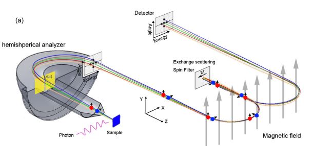
Electron spin plays important roles in determining the physical and chemical properties of matter. However, measurements of electron spin are of poor quality, impeding the development of material sciences, because the spin polarimeter has a low efficiency. Here, we show an imaging-type exchangescattering spin polarimeter with 6786 channels and an 8.5 × 10?3 single channel efficiency. As a demonstration, the fine spin structure of the electronic states in bismuth (111) is investigated, for which strong Rashba-type spin splitting behavior is seen in both the bulk and surface states. This improvement paves the way to study novel spin related phenomena with unprecedented accuracy
-
Fast growth of inch-sized single-crystalline graphene from a controlled single nucleus on
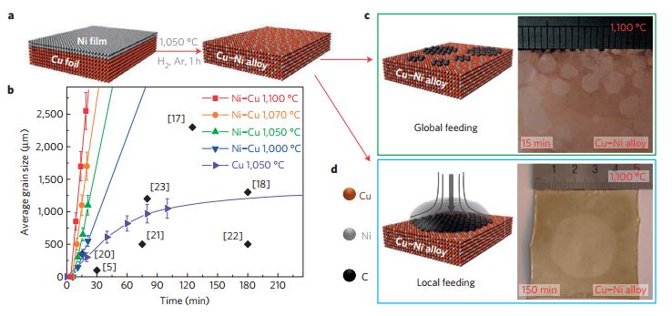
By locally feeding carbon precursors to a desired position of a substrate composed of an optimized Cu–Ni alloy, we synthesized an ~1.5-inch-large graphene monolayer in 2.5 h. Localized feeding induces the formation of a single nucleus on the entire substrate, and the optimized alloy activates an isothermal segregation mechanism that greatly expedites the growth rate5,6. This approach may also prove eective for the synthesis of wafer-scale single-crystalline monolayers of other two-dimensional materials.
-
High-Tc superconductivity in ultrathin Bi2Sr2CaCu2O8+x down to half-unit-cell thickness by protec...

High-T-c superconductors confined to two dimension exhibit novel physical phenomena, such as superconductor-insulator transition. In the Bi2Sr2CaCu2O8+x (Bi2212) model system, despite extensive studies, it is difficult to determine the intrinsic superconducting properties at the thinness limit. Here, we report a method to fabricate high quality single-crystal Bi2212 films down to half-unit-cell thickness in the form of graphene/Bi2212 van der Waals heterostructure, in which sharp superconducting transitions are observed. The heterostructure also exhibits a nonlinear current-voltage characteristic due to the Dirac nature of the graphene band structure.