“Self-Matched” Tribo/Piezoelectric Nanogenerators Using Vapor-Induced Phase-Separated Poly(vinylidene fluoride) and Recombinant Spider Silk
Date:20-03-2020 | 【Print】 【close】
In the era of the Internet of Things (IoTs), sensors, portable electronics, wearable devices, and wireless transport systems are increasing the demand for renewable and green energy supplies. Triboelectric nanogenerators (TENGs) have been actively investigated and extensively developed, aiming for efficiently converting environmental mechanical energy into electricity for powering so-called self-powered sensors or systems. However, some challenges, such as the large internal resistance, the low frictional efficiency, and material inefficiency for losing/gaining electrons, still remain to be overcome before current TENGs can be widely put into practical applications.Recently, a modified concept, known as tribo-piezoelectric nanogenerators (TPNGs), offers an efficient approach to enhance the energy conversion efficiency. This is because the thin-film structure of its active layers in both TENG and piezoelectric nanogenerator (PENG) allows facile integration into desired configurations for specific applications.
Nevertheless, most TPNGs consisting of the tribo and piezoelectric components are based on direct energy superposition. The intrinsic electron-cloud-potentialwell coupling effect of TENG is often overlooked. It is known that the contact and separation of the two pairing tribo-materials generate triboelectrification (or contact electrification). In this process, the charge transfer is affected by the relative capability of gaining or losing electrons, so-called surface-potential difference, which intrinsically depends on the pairing materials themselves. For example, silk proteins readily release electrons after contacting poly(ethylene terephthalate) (PET) because of the huge surface-potential difference between silk and PET. Nevertheless, a recent report shows that the spider silk protein can be genetically engineered to increase such potential difference with PET and be much easier to lose electrons than its natural counterparts. However, for the paired PET and many other materials, there is a lack of effective methods to modify the surface potential. Noticeably, piezoelectric materials can generate surface charge and electron potential under external forces because of the central symmetry breaking of the crystal structure. Therefore, integrating the large surface charge generated by piezoelectric materials could be an effective way to modify the surface-potential difference of tribomaterials. Poly(vinylidene fluoride) (PVDF) is renowned as a good piezoelectric polymer material of simple fabrication and relatively low cost. Furthermore, the excellent flexibility and biocompatibility make PVDF one of the most suitable materials to modify the surface potential of the triboelectric layer.

Figure 1. Design of TPNG using the self-matching approach. a) An electron-cloud-potential-well model proposed to explain the charge transfer between
spider silk and PET with/without PVDF (arrows indicate electron transfer events). b) A schematic model of a TPNG model composed of vapor-induced
phase-separated PVDF (gray dashed box) and regenerated spider silk protein (blue dashed box). c) Molecular models to illustrate the electron transferring
state of the opposite (Tribo“.”Piezo) and accordant (Tribo“+”Piezo) states. d) The voltage signals generated by pure PENG (only PVDF/PET),
TENG (only spider silk/PET), Tribo“.”Piezo, and Tribo“+”Piezo with R = 10 MΩ in series.
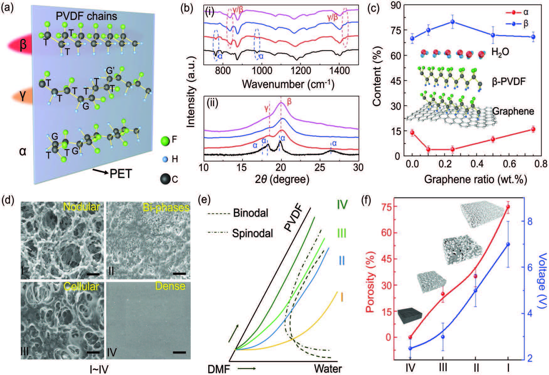
Figure 2. Tuning of matched piezo-PVDF by optimizing piezoelectric phases, doping content, and surface morphologies. a) A 3D model for illustrating
the different configurations of PVDF and their effect on surface-potential differences of PET. (The depth of the color corresponding to the modified
intensity of the PET.) b) The FTIR spectra (i) and XRD results (ii) for: raw powder (black curve), natural-evaporated PVDF membranes (red curve),
phase-separated PVDF film without (blue curve), and with graphene doping (pink curve). c) Deconvolution analyses of the XRD results showing α
and β phase contents with different ratios of graphene doping. d) SEM images of the different morphologies observed in phase-separated PVDF films
(I: nodular; II: bi-phases; III: cellular; IV: dense structures, scale bar, 2 μm). e) Schematic isothermal ternary phase diagram of PVDF/DMF/H2O without
a specific concentration scale. f) The porosity of I–IV structures and associated voltage signals.