Advanced silicon-based materials and applications
Date:09-06-2017 | 【Print】 【close】
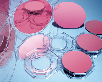
Large scale silicon wafers and SOI wafers are the foundation of integrated circuit manufacturing industry. Due to the advantages of high speed, low power consumption and radiation resistance, etc., SOI is known as the advanced silicon-based material for the nanotechnology era. The State Key
Progress Award (First Prize), etc. Currently, SOI group has about 40 scientific research personnel including 2 academicians of CAS, 13 researchers, 7 associate research fellows and 4 senior engineers, committed to developing advanced SOI-based materials and devices, especially in the areas including: high mobility SOI materials, radiation tolerant SOI materials and silicon photonics.
The main research contents include:
(1) Advanced Si-base substrates: Develop 12 inch silicon wafers and 12 inch fully-depleted SOI wafers to meet the development needs of microelectronics technology along the direction of More Moore. Meanwhile, explore the high mobility SOI materials including sSOI, GOI and GeOI. Develop 8 inch RFSOI wafers and 8 inch power SOI wafers to meet the development needs of microelectronics technology along the direction of More Moore. In addition, explore the hetero-integration of wide-bandgap semiconductor materials such as SiC, GaN, etc. with silicon or SOI base.
(2) SOI KFS chip: SOI technology is an advanced technology that can meet the special application of aerospace environment. Develop special process and technology, implement KFS SOI wafer, and develop highly reliable integrated circuit chip to meet the application requirements of integrated circuit chip in the special environment.
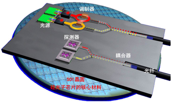
(3) Integrated silicon-based photonic chip: Silicon photonics integrates optical devices and electronics circuits in the same silicon chip using traditional Si manufacturing process. It has achieved data transmission of information, and solved the bottleneck of the interconnection problem of high-performance computers and high-end CPU, etc.
The research goal is to build the global leading silicon wafer production base and provide the source of innovation and the technical support to make it one of the world top 3 wafer vendors. Meanwhile, we are aiming to establish the domestic first-class KFS R&D center, to realize coordinated development of KFZ SOI materials, processes, devices, chips and systems applications, and develop and apply serialized KFZ chip; set up FDSOI technology benchmarking to guide the development of China’s advanced microelectronic process along a differential path, and achieve the important application of FDSOI technology in the fields of internet of things, automotive electronics, etc.
Typical research papers are as follows:
2.How Graphene Islands Are Unidirectionally Aligned on the Ge(110) Surface , Jiayun Dai, Danxia Wang, Miao Zhang, Tianchao Niu, Ang Li, Mao Ye, Shan Qiao, Guqiao Ding, Xiaoming Xie, Yongqiang Wang, Paul K. Chu, Qinghong Yuan,* Zengfeng Di,* Xi Wang, Feng Ding, and Boris I. Yakobson , Nano Letters, 16 (2016) 3160
3.Experimental Demonstration of In-Plane Negative-Angle Refraction with an Array of Silicon Nanoposts , Aimin Wu, Hao Li, Junjie Du, Xingjie Ni, Ziliang Ye, Yuan Wang, Zhen Sheng, Shichang Zou,Fuwan Gan, Xiang Zhang, and Xi Wang , Nano Letters, 15 (2015) 2055
4.Optical Beam Steering Based on the Symmetry of Resonant Modes of Nanoparticles, Dunjie Du, Zhifang Lin, S. T. Chui, Wanli Lu, Hao Li, Aimin Wu, Zhen Sheng, Jian Zi, Xi Wang, Shichang Zou, and Fuwan Gan, Phys. Rev. Lett. 106 (2011) 203903
5.Fluorinated Graphene in Interface Engineering of Ge-Based Nanoelectronics , Xiaohu Zheng, Miao Zhang, Xiaohua Shi, Gang Wang, Li Zheng, Yuehui Yu, Anping Huang, Paul K. Chu, Heng Gao, Wei Ren*, Zengfeng Di* and Xi Wang , Advanced Functional Materials, 25 (2015) 1805
6.Synthesis of Layer-Tunable Graphene A Combined Kinetic Implantation and Thermal Ejection Approach , Gang Wang, Miao Zhang, Su Liu, Xiaoming Xie, Guqiao Ding, Yongqiang Wang, Paul K. Chu, Heng Gao, Wei Ren, Qinghong Yuan*, Peihong Zhang, Xi Wang and Zengfeng Di* , Advanced Functional Materials, 25 (2015) 3666 (Cover paper)
7.Deterministic Assembly of Flexible Si-Ge Nanoribbons via Edge-Cutting Transfer and Printing for van der Waals Heterojunctions , Qinglei Guo, Miao Zhang,Zhongying Xue, Gang Wang,Da Chen,Ronggen Cao,Gaoshan Huang,Yongfeng Mei,* Zengfeng Di* and Xi Wang , Small, 11 (2015) 4044 (Cover paper)
8.Faceted nanostructure arrays with extreme regularity by self-assembly of vacancies, Xin Ou,* Karl-Heinz Heinig, René Hübner, Jörg Grenzer, Xi Wang, Manfred Helm, Jürgen Fassbender, and Stefan Facsko*, Nanoscale, 7 (2015) 18829 (Cover paper)
9.An All-Silicon Passive Optical Diode, Li Fan, Jian Wang,L.T. Varghese, Hao Shen, Ben Niu, Yi Xuan, A. M. Weiner, Minghao Qi , Science 335 (2012) 447
10.Reconfigurable radio-frequency arbitrary waveforms synthesized in a silicon photonic chip, Jian Wang, Hao Shen, Li Fan, Rui Wu, Ben Niu, Leo T. Varghese, Yi Xuan, Daniel E. Leaird, Xi Wang, Fuwan Gan, Andrew M. Weiner, and Minghao Qi , Nature Communications, 6 (2015) 5957
11.Jing Chen*, Jiexin Luo, Qingqing Wu, Zhan Chai, Tao Yu, Yaojun Dong, Xi Wang, A Tunnel Diode Body Contact Structure to Suppress the Floating-Body Effect in Partially Depleted SOI MOSFETs, IEEE Electron Device Letters, 32, (2011) 1346
12.Qingqing Wu, Jing Chen*, Zhichao Lu, Zhenming Zhou, Jiexin Luo, Zhan Chai, Tao Yu, Chao Qiu, Le Li, Albert Pang, Xi Wang, and Jerry G. Fossum, Experimental Demonstration of the High-Performance Floating-Body/Gate DRAM Cell for Embedded Memories, IEEE Electron Device Letters, 33, (2012) 743
13.Kai Lu, Jing Chen*, Jiexin Luo, Jun Liu, Qingqing Wu, Zhan Chai, and Xi Wang, Improvement of RF Performance by Using Tunnel Diode Body Contact Structure in PD SOI nMOSFETs, IEEE Electron Device Letters, 35, (2014) 15