RESUME
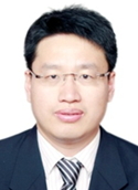
Xin Ou, Professor of Shanghai Institute of Microsystem an Information Technology (SIMIT). He graduated from the department of material science of HeiFei university of technology (2006, Bachelor), ZheJiang University (2006, Master) and Chinese academy of science (2009, Ph.D.) From 2007 to 2009, He studied in German research center of Dresden-Rossendorf as a joint-Ph.D. student. After that, He served as a postdoctorate fellow and scientist in Max plank institute for solid state research (2009-2010) and Helmholtz Zentrum Dresden-Rossendorf (2010-2014). In 2015, He was appointed as a full professor in SIMIT, Chinese Academy of Science. Currently, he leads a research group working on the advanced SOI materials, heterogeneous Integration and nanofabrication. Dr. Xin Ou has published 50 journal papers and contributed to 2 book chapters. He has delivered 10 invited speeches and 24 oral talks at international conferences.
education
2010.3 Doctor degree of engineering was issued on 1st Mach, 2010
2006-2009 Ph.D. of Chinese Academy of Sciences, China
2003-2006 Postgraduate in Material Science and Engineering, Zhejiang University, Hangzhou, China.
1999-2003 Bachelor degree in Material Science and Engineering, HeFei University of Technology, He Fei, China.
work experience
2014-the present Professor, Shanghai Institute of Microsystem and Information Technology, Chinese Academy of Sciences, China.
2010-2014 Research scientist and Posdoc. researcher, Institute of Ion Beam Physics and Materials Research at theHelmholtz-Zentrum Dresden-Rossendorf (HZDR), Germany.
2009-2010 Posdoc. researcher, Max Planck Institute of Microstructure Physics in Halle (Germany) and Guest scientist at Forschungszentrum Dresden-Rossendorf, Germany.
HONORS AND AWARDED RESEARCH FUNDS
1. "BMM”prize granted by the international committee of 20th International Conference on Ion Beam Modification of Materials.
2. "National Science Fund for Outstanding Youth Scholars” for the achievements in the research: Ion beam fabrication and modification of materials for informatics, Fund 1.5 Million Yuan (2016)
3. “One-Hundred talent program” of Chinese Academy of Science, Fund 3.3 Million Yuan (2015)
4. “Pujiang talent program” of Shanghai Government, Fund 0.2 Million Yuan (2013)
5. “EMRS Best Poster Award” granted by European Materials Research Society Conference, 27-31.05.2013, Strasbourg, France (2013)
6. “2010 Research Award” of Helmholz-Zentrum Dresden-Rossendorf, Germany. This is the annual award of German Helmholtz HZDR research center (2011)
7. “Excellent Doctoral Thesis Award” Granted by Chinese Academy of Science (2011)
8. “Young Investigator Award” granted by 18th International Conference on Ion Implantation Technology (IIT 2010), 2010, Kyoto, Japan (2010)
9. “Graduate Outstanding Achievements (Thesis)” Granted by Shanghai Government. (2011)
SELECTED PUBLICATIONS
1.X. Ou*, K.H. Heinig, R. Hubner, J. Grenzer, X. Wang, M. Helm, J. Fassbender, S. Facsko*, Faceted nanostructure arrays with extreme regularity by self-assembly of vacancies, Nanoscale 45, 18928 (2015).
2. T.You, X. Ou*, G.Niu, F. Bärwolf, G. Li, N. Du, D. Bürger, I. Skorupa, Q. Jia, W. Yu, X.Wang, O.G. Schmidt, and H.Schmidt, Engineering interface-type resistive switching in BiFeO3 thin film switches by Ti implantation of bottom electrodes, Scientific Reports 5, 18623(2015).
3. X. Ou, A. Keller, M. Helm, J. Fassbender, S. Facsko Reverse epitaxy of Ge: ordered and facetted surface patterns,Physical Review Letters 111, 016101(2013).
4. X. Ou*, Y. Shuai, W. Luo, P.F. Siles, R. Kögler, J. Fiedler, H. Reuther, S. Zhou, R. Hübner, S. Facsko, M. Helm, T. Mikolajick, O. G. Schmidt, H. Schmidt, Forming-free resistive switching in multiferroic BiFeO3 thin films with enhanced nanoscale shunts, ACS Applied Materials & Interfaces 5:23, 12764-12771 (2013).
5. Y. Shuai, X. Ou* W. Luo, A. Muecklich, D. Buerger, S. Zhou, C. Wu, Y. Chen, W.L. Zhang, M. Helm, T. Mikolajick, O.G. Schmidt, H. Schmidt Key concepts behind forming-free resistive switching incorporated with rectifying transport properties, Scientific Reports 3:2208 (2013).
6. Y. Shuai, X. Ou*, N. Du, C. Wu, W.L. Zhang, D. Buerger, C. Mayr, R. Schueffny, S. Zhou, M. Helm, H. Schmidt Nonvolatile multilevel resistive switching in Ar+ irradiated BiFeO3 thin films, IEEE Electron Device Letter 34, 1 (2013).
7. X. Ou*, R. Kögler, H.B. Zhou, W. Anwand, J. Grenzer, R. Hübner, M. Voelskow, M. Butterling, S. Zhou, W. Skorupa, Release of helium from vacancy defects in yttria-stabilized zirconia under irradiation, Physical Review B 86, 224103 (2012).
8. X. Ou*, Nadine Geyer, R. Kögler, P. Werner, W. Skorupa, Acceptor deactivation in individual Si nanowires: from thick to ultrathin, Applied Physics Letters 98, 253103 (2011).
9. X. Ou*, P.D. Kanungo, R. Kögler, P. Werner, U. Gösele, W. Skorupa, and X. Wang
Three-Dimensional Carrier Profiling of Individual Si Nanowires, Advanced Materials 22, 4020-4024 (2010).
10. X. Ou*, P.D. Kanungo, R. Kögler, P. Werner, U. Gösele, W. Skorupa, and X. Wang Carrier Profiling of Individual Si Nanowires by scanning spreading resistance microscopy, Nano Letters 10 (1), 171-175 (2010).

