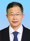
RESUME
EDUCATION
1980-1990 Chemical and Electrical Engineering
Ph.D. of Electrical Engineering, Yale University
M.S. of Chem. Engineering, Yale University
B.S. of Chem. Engineering,
WORK EXPERIENCE
8/2002–Now
Vice President of R&D
§ 0.25um Flash manufacturing ramp in Yasu and HHNEC
§ 0.18um JDP in TSMC, Vanguard, Samsung and GSMC
§ 0.11um JDP for 2Gb Media JDP in
Chalcognide JRP with SiMIT/Fudan Univ./SJTU
8/2000–7/2002 IBM Micro. Division East
Senior Manager of R&D Function (3rd level)
§ Advanced unit process development of DRAM and Foundry-ASIC
Early Production and tech-transfer of DRAM and Foundry-ASIC
12/1997–7/2000 IBM Micro. Division
IBM-Infineon JDP of 0.18um/0.13um/90nm technology for Foundry/SoC
11/1997-10/1994 IBM Micro. Division East
Manager of (1st level) department
§ IBM-Toshiba JV : 64Mb/256Mb new fab-construction and tech-transfer
§ IBM Research : 0.25um research project under DARPA grand of
8/1990-9/1994 IBM Micro. Division
§ Lead integration engineer in 256Mb DRAM (East
§ Lead integation engineer in 0.7um BiCMOS for AS400 (Burlington, VT)
Mid-of-line module engineer in 0.7um CMOS for RS6000 (BTV, VT)

